LUMINA is a European research and innovation project developing a new generation of ultra-high-speed, low-power photonic and optoelectronic technologies for future communication networks. By combining graphene, electro-optic polymers, and advanced photonic integration, LUMINA aims to overcome the performance and energy limitations of today's telecom infrastructure. The project targets breakthrough devices including modulators, photodetectors, and optoelectronic mixers with bandwidths exceeding 500 GHz. These technologies will be integrated into scalable, CMOS-compatible photonic platforms and demonstrated in real-world wireless and optical communication scenarios for future data centers and 6G networks.

About
Vision
LUMINA envisions a future where communication systems can sustain exponentially growing data traffic without increasing their environmental footprint. By unlocking the potential of innovative advanced materials, the project seeks to redefine how photonic integrated circuits are designed, manufactured, and deployed. The long-term vision is to enable terabit-scale wireless and optical communications that combine extreme bandwidth, low energy consumption, compact footprints, and industrial scalability. Through a fully European value chain and advanced manufacturing ecosystem, LUMINA aims to strengthen Europe’s leadership in next-generation photonics and communication technologies.
Keyfacts
Reference
Reference Number:
101298684
Programme type:
HORIZON-RIA
Programme acronym:
HORIZON-CL4-2025-03
Duration
Project Start:
01.09.2026
48 Months
Cost and Funding
Costs: € 4.814.297,50
Funding: € 4.814.294,50
Motivation
The world’s digital infrastructure faces a growing challenge: data traffic is increasing dramatically, driven by AI, cloud computing, immersive applications, and future 6G services. At the same time, communication networks and data centers already consume significant amounts of energy, creating both economic and environmental pressures. Existing photonic technologies struggle to simultaneously deliver higher speeds, lower power consumption, and scalable manufacturing. LUMINA addresses this gap by exploring disruptive material platforms such as graphene and electro-optic polymers, which offer unique opportunities to achieve unprecedented bandwidth, energy efficiency, and integration density for future telecom systems.
Mission and Objectives
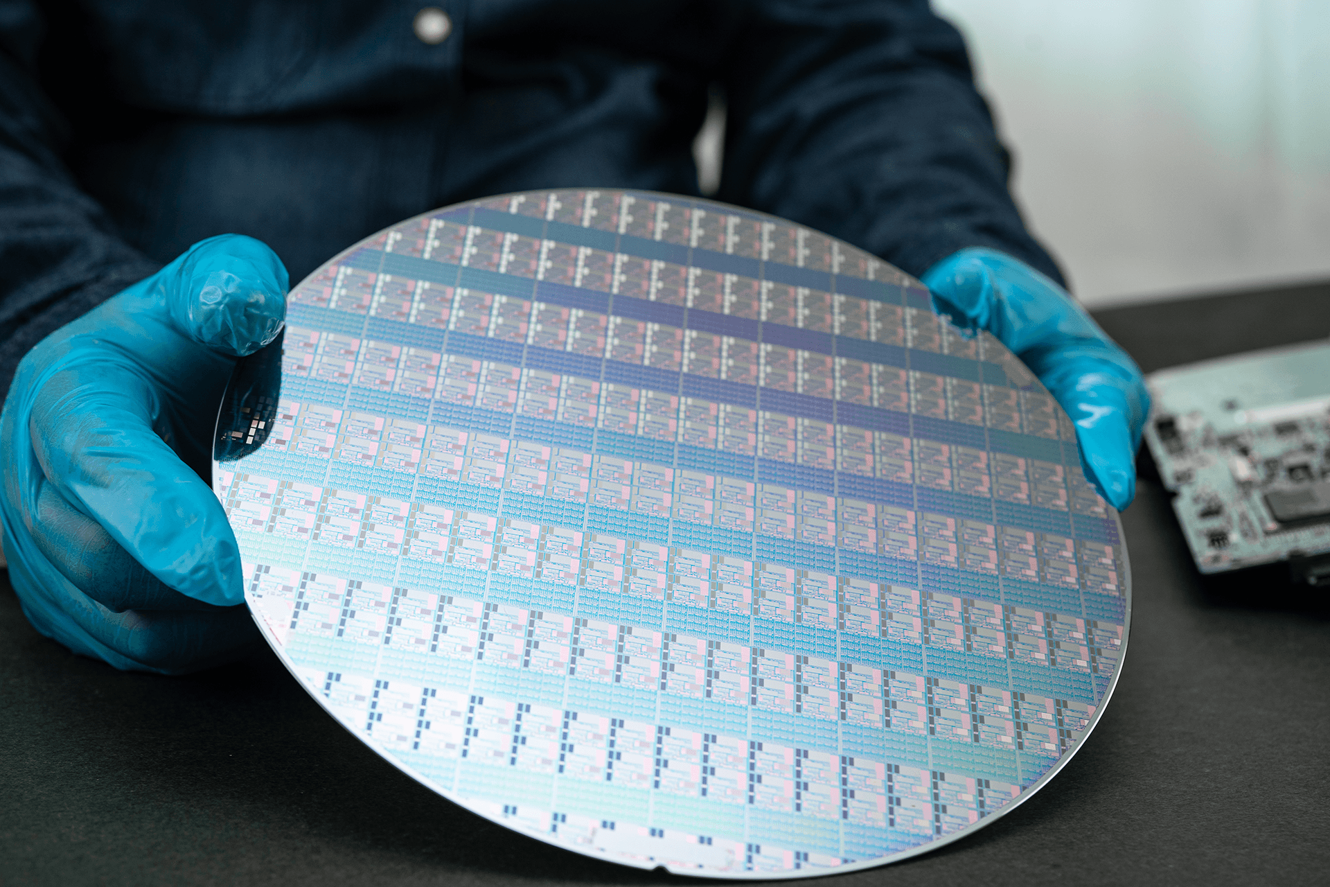
LUMINA’s mission is to demonstrate that innovative advanced materials can enable a new class of high-performance photonic devices for future communication systems. The project will develop ultra-fast modulators, graphene-based photodetectors, and optoelectronic mixers capable of operating at bandwidths up to and beyond 500 GHz. It will also establish scalable wafer-level integration processes, advanced packaging technologies, and low-loss optical interconnects compatible with industrial manufacturing. These developments will culminate in fully integrated prototype transmitters and receivers for wireless 6G and optical data-center applications, validated under realistic operational conditions and advanced to TRL6 readiness.
- Demonstrate EO polymer-based ultra-high-speed, low power consumption, low footprint modulators
- Demonstrate high bandwidth, low power consumption graphene-based optoelectronic mixers with state-of-the-art conversion efficiency
- Demonstrate graphene-based ultra-high-speed and high responsivity photodetectors
- First hybrid integration on wafer-scale of graphene, EO polymers and Al-based plasmonic resonators
- Demonstrate low-losses optical interconnect thanks to additive manufacturing of polymer-based freeform optics
- First integration and packaging of prototypes with a 500GHZ RF bandwidth
Work Packages
WP1
System definition and prototype design
01.09.2026
28.02.2029
Detailed information
WP1 will analyse use case scenarios to determine key system requirements and drive the overall design. It will define the high-level system architecture, specifications, and sub-systems, and translate these into detailed module designs, including individual component characteristics and required performance levels. This WP ensures that all subsequent development activities are aligned with the project’s objectives and system-level targets.
WP2
IAM-based component development
01.09.2026
31.08.2028
Detailed information
The objective of this work package is to develop and demonstrate the core IAM-based devices that underpin the sub-systems defined in WP1. We will design, fabricate, and characterize high-speed and low-loss modulators, graphene modulators and mixers, ultrafast graphene photodetectors, tuneable ring resonator filters, and broadband dielectric RF phase shifters. Their performance will be benchmarked against the state of the art and continuously fed back to WP1 to enable system-level integration (OBJ 1-4).
WP3
Wafer-scale fabrication
01.09.2026
31.08.2030
Detailed information
Process development and fabrication of 3 main wafer runs for all the sub-systems. This includes all test substrates for WP2, including these for sample scale fabrication using Au plasmonics at ETH, and transitioning this technology to wafer scale CMOS-compatible Al plasmonics in WP3 (OBJ 1, 3, 4).
WP4
Assembly and Packaging technologies for IAM devices
01.08.2027
31.05.2030
Detailed information
To develop the control electronics and the device’s control algorithms. To integrate all the developed PICs (WP3) in an ESD-free, thermally controlled environment, ensuring stable operation. The final prototype will be able to operate in a relevant environment (TRL-6) (OBJ 6, 7).
WP5
System and prototypes characterisation and demonstration
01.08.2028
31.08.2030
Detailed information
This WP objectives are to offer feedback to the other WP to ensure optimum performances in the last prototypes, and to demonstrate the project prototypes in TRL6 conditions (OBJ 6, 7).
WP6
Project, Risk, and Innovation Management
01.09.2026
31.08.2030
Detailed information
WP6 is responsible for the operational management and technical vitality of the LUMINA project encompassing management tasks on contractual, financial, legal, technical, and administrative levels.
WP7
Communication, Dissemination, Exploitation and Standardisation
01.09.2026
31.08.2030
Detailed information
This Work Package is dedicated to LUMINA’s communication, dissemination, exploitation, and standardisation activities, ensuring that the project achieves maximum visibility, uptake, and long-term impact.
